
Explore Our X-ray Solutions
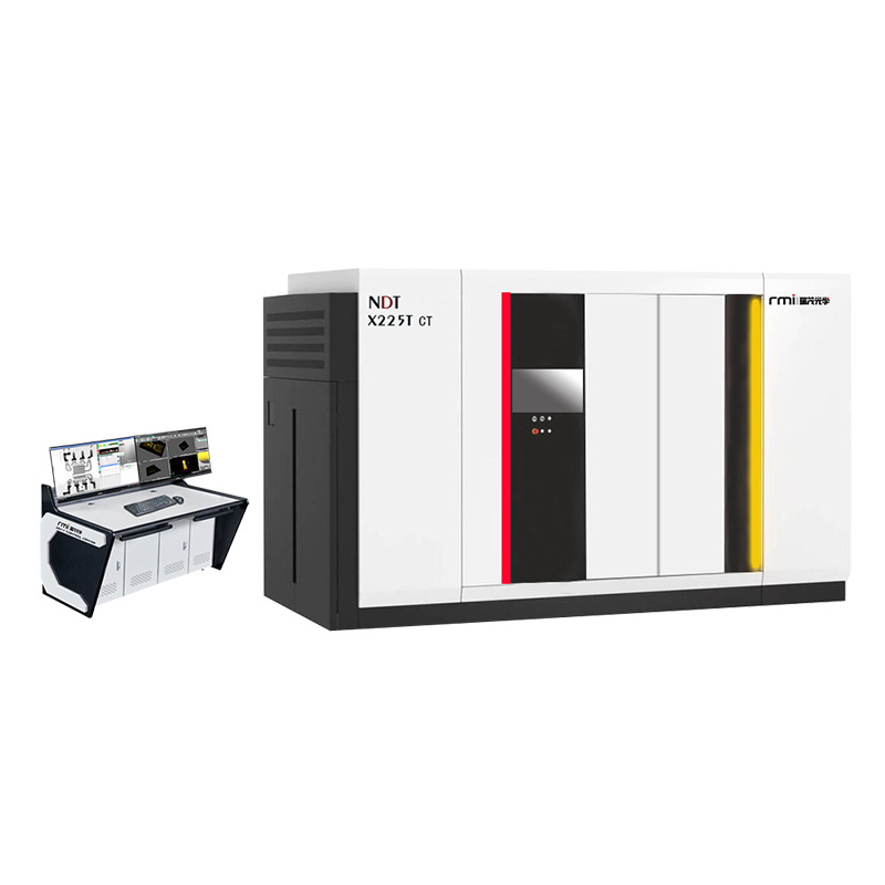
x-225CT
The X-225T-CT is designed for non-destructive inspection of aluminum castings, detecting internal defects such as cracks, shrinkage porosity, gas pores, and sand holes. Its CT imaging capability enables detailed evaluation of complex and safety-critical components, helping manufacturers ensure quality and reduce rejection losses.
- X-ray Voltage: 160KV
- Spatial Resolution: 50μm
- Detector: 3072x3072px
- Inspection Size: Maximum Diameter 870mm
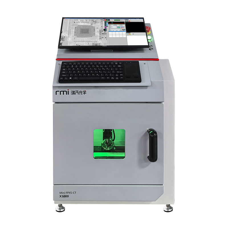
X-3000M
The X-3000M is primarily used for inspecting the drilling alignment of PCB boards. Featuring high gain, high sensitivity, high spatial resolution, and a fast response time, this model is widely recognized and well received by customers.
- X-ray Voltage: 90KV/ 80KV
- Spatial Resolution: 5-7μm/10-15μm
- Detector: 1536*1536px
- Inspection Area: 130x130mm
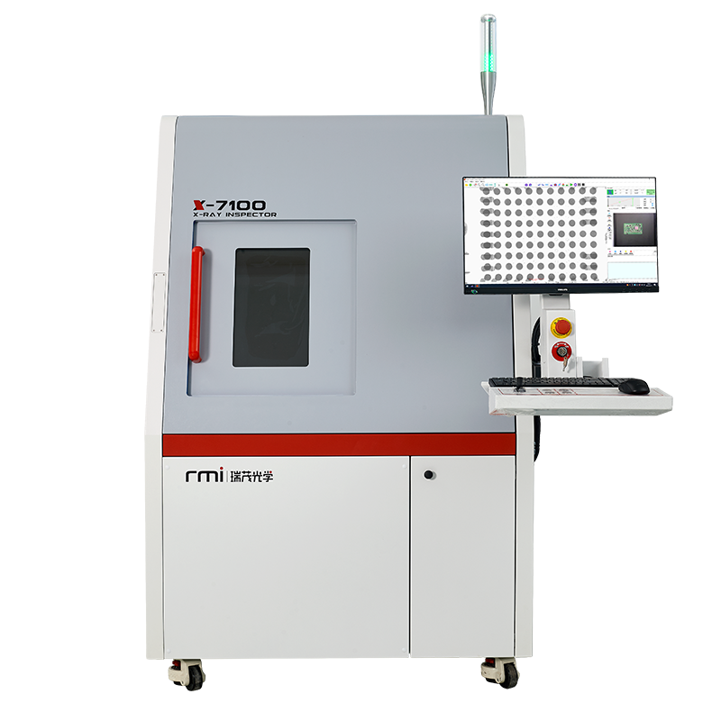
X-7100
A general-purpose X-ray inspection system for internal structure inspection of electronic components, solder joints, circuits and industrial samples, supporting 60° oblique observation and automated batch inspection functions.
- X-ray Voltage: 90KV
- Spatial Resolution: 5μm
- Detector: 1536x1536px
- Inspection Area: 510x510mm
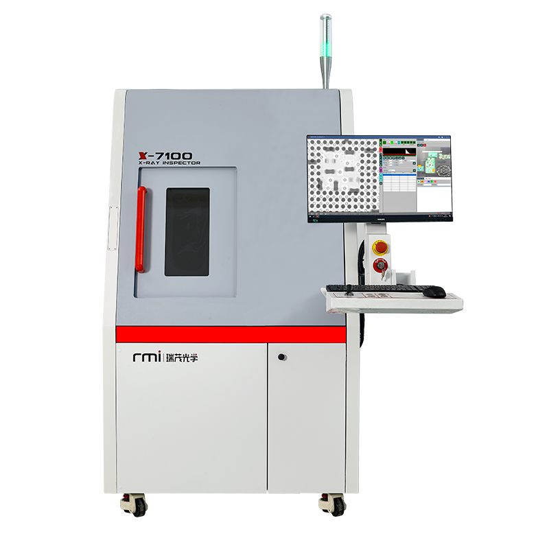
X-7100 (mini)
The X-7100 X-ray inspection system has a wide range of applications. It is commonly used to inspect the internal structures of electronic components, including void-rate measurement, circuit short-circuit and open-circuit detection, insufficient or missing solder joints, foreign objects, and internal cracks.
- X-ray Voltage: 90kv
- Spatial Resolution: 5μm
- Detector: 1536*1536px
- Inspection Area: 510x370mm
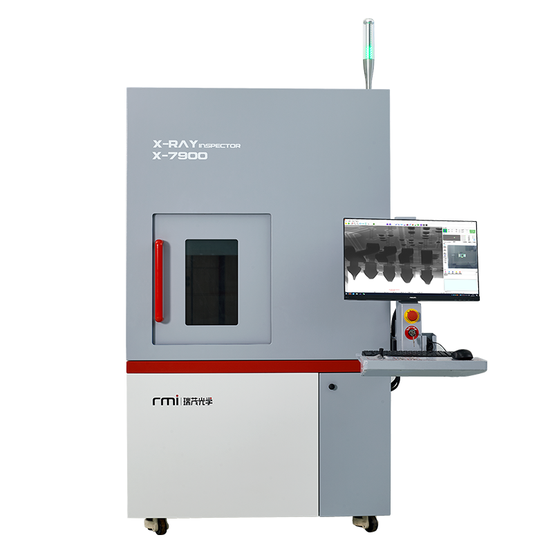
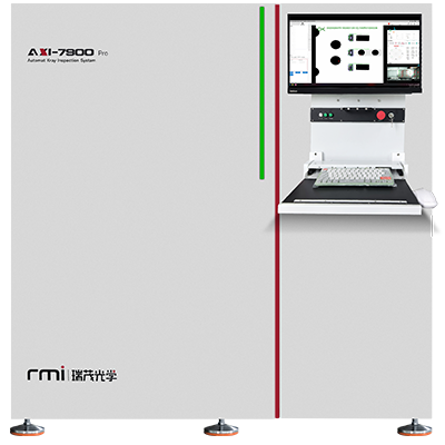
X-7900
The X-7900 semiconductor X-ray inspection system can detect defects as small as 3 μm. It supports one-click measurement of void size and void ratio, with up to 400× geometric magnification and 2,500× image-system magnification.
- X-ray Voltage: 130kv
- Spatial Resolution: 5μm
- Detector: 1536x1536px
- Inspection Area: 510x510mm
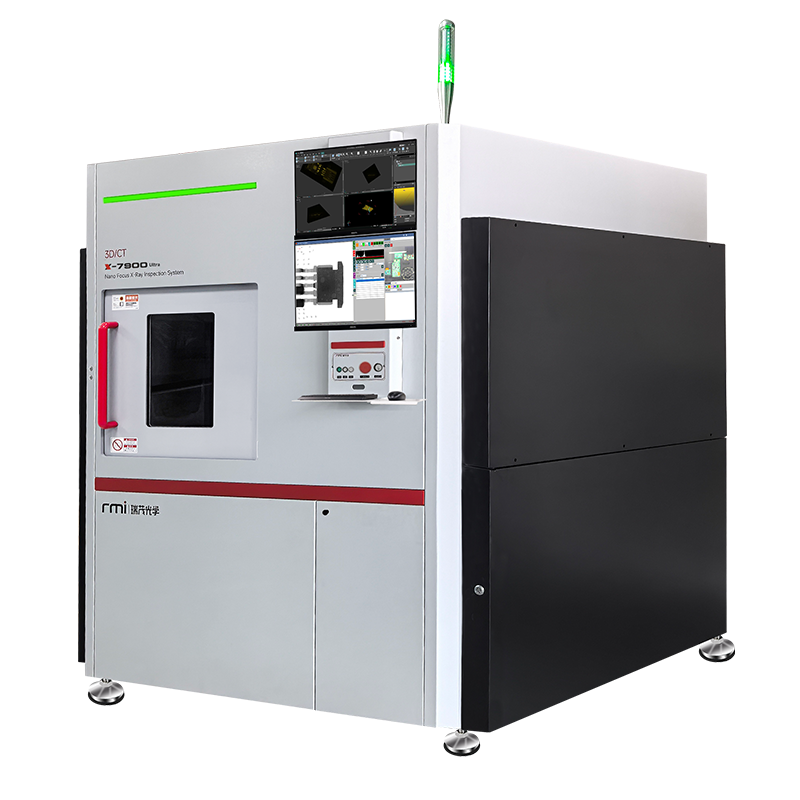
X-7900 Ultra (3d/ct)
X-7900 ultra (3D/CT) Semiconductor Inspection System features a minimum detection accuracy of 1μm and is used for high-precision testing of integrated circuit chip semiconductors, such as BGA, IGBT, flip-chip,PCBA component soldering, LED bonding, IC packaging.
- X-ray Voltage: 160KV
- Spatial Resolution: 1μm
- Detector: 1536x1536px
- Inspection Area: 600x600mm